
Physicists could justly be accused of living in a bit of a fantasy world. As every student encountering physics for the first time knows, very little gets done unless we assume that friction does not exist, objects are perfectly shaped blocks or balls, and collisions release no energy in the form of sound or heat. Of course the real world doesn’t work this way, which is why one role of an experimental physicist is to investigate complicating effects that can’t be easily understood with mathematical tools. In this post, we’ll take a look at a recent effort to understand one such complicating effect by Dr. Xiaoqing Pan’s materials science research group.
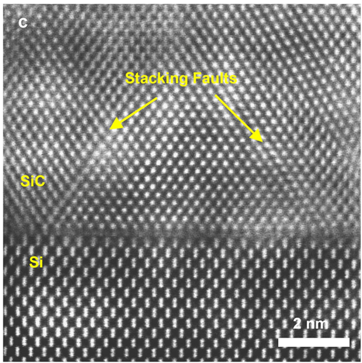
Generally speaking, the aim of materials science is to understand the properties of matter, especially solids. Many solids have crystal structure, which means the atoms are arranged in a repeating pattern. Similar to assuming friction does not exist as you may have done in physics class, a common simplifying assumption in materials research is that the crystal is perfect. This means not a single atom is out of place, and the pattern repeats onward forever and ever. Of course, this is never really the case. Beyond the obvious problem that the lattice can’t go on forever, crystals in the real world usually come with defects. Rather than a perfect pattern of atoms, every now and then the atoms arrange themselves into a different crystal structure in a small part of the material. There are many different kinds of defects in different types of materials, but Dr. Pan’s group was particularly interested in stacking fault defects in silicon carbide (SiC) crystals. These stacking faults are believed to play an important role in determining the ability of SiC crystals to conduct heat. SiC is a commonly used semiconductor for making electronics, so understanding these defects and how they affect the crystal’s conductive properties is an important practical question. An image of an SiC crystal is shown in the figure. Each of the dots in this image are individual atoms. For an idea of the scale, the 2 nano-meter bar in the bottom right is roughly equal to the diameter of a single strand of DNA. If you look closely, you will see the stacking faults as a slight misalignment of the atoms at the points labeled by the yellow arrows. Just as the addition of friction makes a standard physics problem more difficult to solve, these defects can’t be easily accounted for using the standard mathematical tools physicists use to describe crystal structures. However, we can still learn about them by performing experiments in the real world and measuring their effects on the material.
The Pan group’s experiment hinged on two complementary techniques for studying crystal properties, known as Scanning Transmission Electron Microscopy (STEM) and Electron Energy Loss Spectroscopy (EELS). While the details of these techniques are complicated, their uses in this experiment are conceptually simple. STEM can be used to find defects, and EELS is used to measure the vibrational properties of the material. It was previously unknown how defects in the crystal modify these vibrational properties, so the researcher’s goal was to use EELS to measure the vibrational properties around a stacking fault. This may sound like an easy problem to solve: simply find a stacking fault and then apply EELS. However finding these faults requires applying STEM to image the crystal lattice on the level of individual atoms, and EELS requires its own experimental setup which picks out different vibrational modes in the crystal. Since both techniques are challenging, no one had ever used EELS to measure the vibrational properties of a crystal around a stacking fault until this experiment.
The crucial innovation of Dr. Pan’s group was to adapt the state-of-the-art STEM and EELS techniques for both high spatial resolution imaging and high momentum resolution vibrational measurements. Fundamentally both techniques rely on passing a beam of electrons through the crystal, so they can both be constructed around the same electron beam. However, STEM imaging requires the electrons are used to accurately infer the positions of atoms in real space, while EELS requires the electrons are used to accurately infer the vibrational properties present in the reciprocal space. Unfortunately, these two uses of the electrons are mutually exclusive, meaning using the electrons to measure position accurately makes it difficult to measure individual vibrational states accurately, and vice versa. The researchers were able to get around this issue by constructing an apparatus that could continuously tune this trade off between accurately measuring position and accurately measuring vibration. This means the same apparatus could apply either STEM imaging or EELS just depending on some tunable properties of the electron beam. Once all of this complicated instrumentation was in place, they could do a conceptually simple experiment that had never been done before. First, they configured the electron beam to apply STEM imaging and find a stacking fault in the crystal. Once the beam was positioned above a stacking fault, they tuned the beam to another setting and applied EELS to measure the vibrational properties around a stacking fault.
The first ever measurement of a defect amplifying a vibration in a crystal
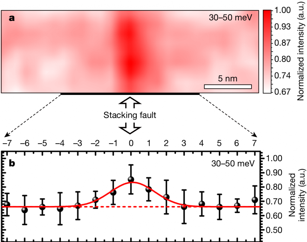
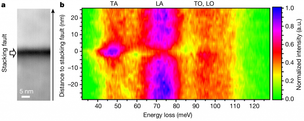
What the experimenters found in their EELS data was a never before measured enhancement of a particular type of vibration in the crystal around the stacking fault. When the intensity of a particular vibration is plotted against the distance from the stacking fault, you see a very clear bump in the intensity, representing an amplification in this particular vibrational mode (see figure above). Interestingly, this increase in intensity is specific to only one type of vibration. Crystals have different types of vibrations that can propagate through the lattice. Physicists call these vibrations “phonons”, and categorize these vibrations based on how they propagate through the crystal. In the figure below, you can see a plot which separates 4 different types of phonons, labeled using the initials above the plot. Here, the distance to the stacking fault is plotted on the vertical axis, where the stacking fault forms a horizontal line across the middle of the figure. Note that right in the middle of the figure, or at the stacking fault, the TA (or transverse acoustic) vibration is amplified as the color turns deep blue, which is high intensity. Further, the LA (or longitudinal acoustic) vibration is actually suppressed by the stacking fault. All of these effects have never been seen before. However after the researchers had completed the experiment, they became aware of a theoretical paper that predicted something like the shifts in the vibrational properties that they had seen. Those theoretical predictions offered additional support to the group’s findings, but as UCI post-doc Xingxu Xan puts it, “seeing is believing”, meaning only after these effects were seen in an experiment could they be considered newly discovered physics.
In the future, Dr. Pan’s group hopes that the new technique of combining STEM and EELS can help us understand the effect of defects in many other types of materials. The vibrational properties of a material determine how thermal energy flows from one part of the material to the other, which has important consequences for designing new electronics, medical devices, or really any technology that makes use of materials with a particular crystal structure. The group also has plans to improve their experimental setup to make even more previously impossible measurements. Studying materials at the nanoscale, that is, on the level of individual atoms, is both fascinating in its own right and has many important applications in making designer materials for new technologies. This new way of understanding crystals with complicating defects is an important new tool in the burgeoning field of materials science.
Post by Kevin Greif, a graduate student at UCI
Edited by Astrid Anker, Xingxu Yan
- Yan, X., Liu, C., Gadre, C. A., Gu, L., Aoki, T., Lovejoy, T. C., Dellby, N., Krivanek, O. L., Schlom, D. G., Wu, R., & Pan, X. (2021). Single-defect phonons imaged by electron microscopy. Nature, 589 (7840), 65–69. https://doi.org/10.1038/s41586-020-03049-y
- Li, M., Ding, Z., Meng, Q., Zhou, J., Zhu, Y., Liu, H., Dresselhaus, M. S., & Chen, G. (2016). The Non-Perturbative Quantum Nature of the Dislocation-Phonon Interaction. Nano Letters, 17 (3), 1587–1594. https://doi.org/10.1021/acs.nanolett.6b04756